Blog
Posts on systems and tools.
A small set of technical posts. Mostly things I have had to understand carefully enough to explain back to myself.
What Makes a Lens "Meta"?
A short introduction to metalenses, metasurfaces, and the nanofabrication steps needed to make flat optics work.
Read the post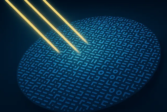
-
 The Semiconductor Trifecta: Understanding Intel, TSMC, and ASML's Interconnected Roles
 -
 How 2D Materials are Changing Lithography and Semiconductor Manufacturing
 -
 Real-time Data Processing in AFM
 -
 The Agile Hardware-Software Balance
 -
 Applying the Observer Software Design Pattern in Nanolithography Tools
 -
 The Intersection of AI and Nanotechnology
 -
 USB3 vs Ethernet: A Comparison of Communication Protocols
 -
 Navigating Precision: Exploring Positioning Systems in Micro and Nano Lithography Tools
 -
 User Interfaces: Scientific Machines vs General Purpose Applications
 -
 Substrate Preparation in Nanolithography: The Foundation for Precision
 -
 PLCs: Workings, Applications, Limitations
 -
 Understanding FPGAs and Their Distinction from CPUs
 -
 Nanolithography: Techniques, Challenges and Future Directions