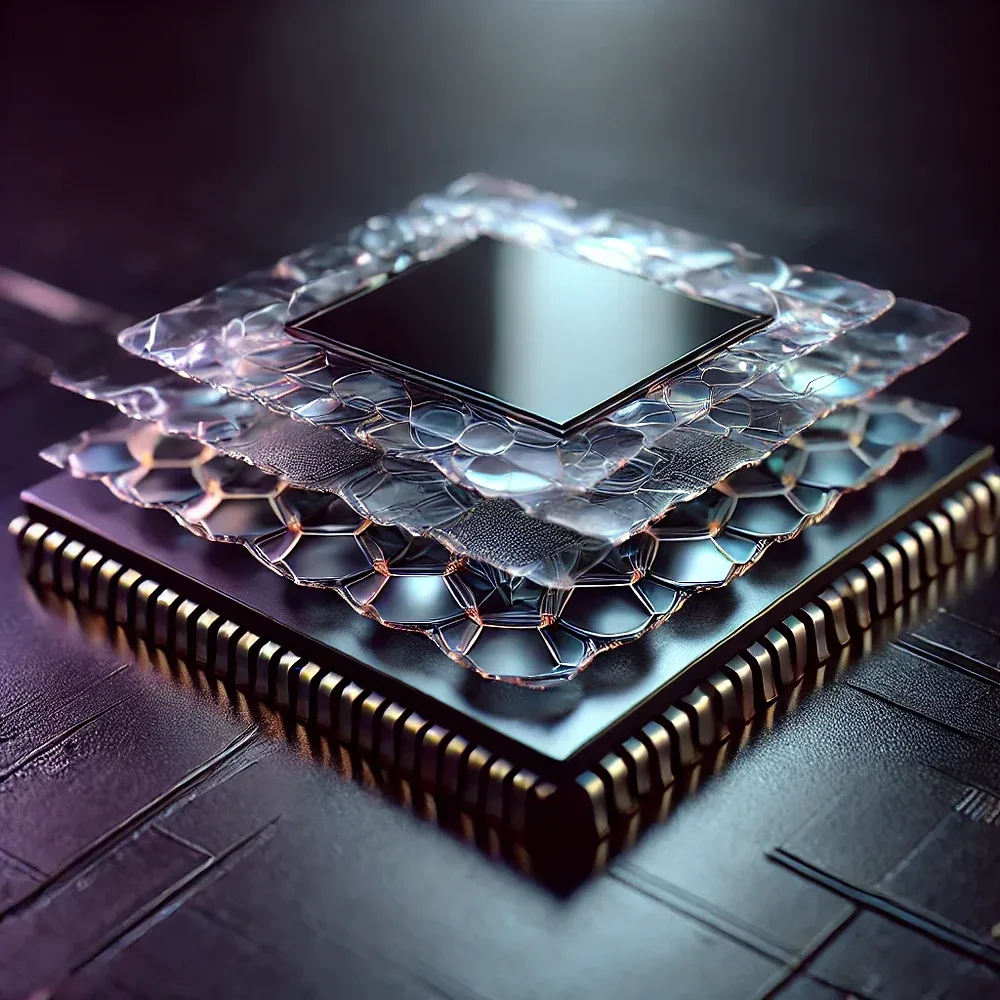
The semiconductor industry is reaching a critical point. As we push silicon-based technology to its limits, finding new materials to keep up with the pace of innovation has become essential. That is where two-dimensional (2D) materials come into play: a group of incredibly thin materials that could reshape electronics and related fields.
Integrating 2D materials is one of the most exciting and challenging developments. In this post, I will explore what 2D materials are, how they are impacting lithography, and how software development helps advance this technology.
Understanding 2D materials
2D materials are crystals made up of a single layer of atoms. This extreme thinness gives them unique properties that differ from thicker materials. The most well-known is graphene, a single layer of carbon atoms arranged in a honeycomb pattern. Discovered in 2004, graphene is strong, lightweight, and an excellent conductor of electricity.
But graphene is not the only 2D material of interest:
- Transition Metal Dichalcogenides (TMDs): Materials like molybdenum disulfide (MoS2) act as semiconductors suitable for transistors and sensors.
- Hexagonal Boron Nitride (h-BN): Known as “white graphene,” h-BN is a good insulator and has high thermal conductivity, making it useful for substrates and insulating layers.
- Phosphorene: A single layer of black phosphorus with adjustable electronic properties, promising for flexible electronics.
By stacking different 2D materials, we can create structures with customized properties, which is challenging to achieve with traditional materials.
Potential applications
2D materials could lead to several advancements:
- New transistors: As silicon transistors near their scaling limits, 2D materials like MoS2 offer a way to make even smaller and more efficient transistors.
- Flexible electronics: Their thinness and flexibility make 2D materials ideal for devices that can bend or fold, such as flexible screens or wearable sensors.
- Quantum computing: Some 2D materials have special properties useful for quantum computers.
- Improved energy devices: They might enhance batteries and solar cells, leading to better energy storage and conversion technologies.
However, incorporating these materials into manufacturing processes presents challenges, especially in fabrication and integration.
The role of lithography
Lithography is crucial in making semiconductors. It is how we create tiny patterns on chips. With 2D materials, this process becomes even more delicate because the materials can be only one atom thick, so minor defects can cause significant problems.
Some key challenges include:
- Surface preparation: The substrate must be extremely clean because contaminants can affect the 2D material’s properties.
- Layer alignment: Precise alignment within a few nanometers is necessary, requiring advanced software and control systems.
- Material compatibility: Standard materials and methods might damage 2D materials, so new approaches are needed.
- Etching and deposition: These processes must be controlled carefully to avoid introducing defects.
How software helps
Software plays a vital role in tackling these challenges.
Simulation and modeling
Advanced software can simulate the lithography process at the atomic level. This helps predict how 2D materials will behave during fabrication, allowing adjustments before making actual devices.
For instance, simulations can show how MoS2 reacts to different light wavelengths during lithography, helping teams fine-tune the process.
Machine learning
Machine learning algorithms can analyze large amounts of data from the fabrication process to find patterns and optimize settings. They can adjust parameters in real time to reduce defects.
Real-time control
By integrating sensors with software, fabrication systems can make adjustments during processing. If a misalignment is detected, the software can correct it immediately, which is crucial for building sensitive devices like quantum components.
Looking ahead
Scaling up the production of 2D materials is a significant challenge. Techniques like Chemical Vapor Deposition (CVD) allow for larger-scale synthesis but introduce new variables that software needs to manage.
Integrating 2D materials into existing manufacturing processes also requires compatibility at every step. Software is crucial because it provides the flexibility and precision needed.
In the future, I anticipate developments such as:
- Combining materials: Using both 2D materials and traditional semiconductors to create hybrid devices.
- Discovering new materials: Employing AI to predict and create new 2D materials with desired properties.
- Enhanced fabrication: Implementing faster data processing and decision-making within fabrication equipment.
Conclusion
Integrating 2D materials into semiconductor manufacturing has the potential to redefine technology. Achieving this depends on innovation in both lithography and the software that controls it.
As a software engineer in this field, I am excited to be part of a journey that combines physics, materials science, and engineering. While there are challenges, the potential benefits make it worthwhile. We are not just making devices smaller or faster; we are building the foundation for future technologies that could significantly impact society.
Recommended resources
- Geim, A.K., and Novoselov, K.S. (2007). “The rise of graphene.” Nature Materials, 6, 183-191.
- Chhowalla, M., et al. (2013). “The chemistry of two-dimensional layered transition metal dichalcogenide nanosheets.” Nature Chemistry, 5, 263-275.
- Rogers, J.A., Someya, T., and Huang, Y. (2010). “Materials and mechanics for stretchable electronics.” Science, 327(5973), 1603-1607.
- Xie, W., and Cao, G. (2021). “Machine learning for 2D material discovery.” Journal of Materials Science & Technology, 83, 113-121.