
What Makes a Lens “Meta”?
- Kartik Buddha
- Jul 27, 2025
- 3 min read

Understanding the Physics and Fabrication of Metalenses
Why do all the lenses we know — from microscope objectives to DSLR cameras — look like little curved pieces of glass? And more importantly: do they have to?
This question has given rise to a fascinating class of optical elements called metalenses — lenses that don’t bend light with curvature, but with structure. Imagine a lens that's completely flat but still focuses light better than some of the best traditional optics. That’s the promise (and the puzzle) of metalenses.
Let’s unpack what makes a lens “meta,” what’s actually happening at the nanoscale, and how we’re learning to make them — one nanopillar at a time.
The Optical Illusion of a Flat Lens
To appreciate the magic of metalenses, let’s start with what a conventional lens does. Traditional lenses rely on the principle of refraction: light changes direction as it passes through a curved interface between two media (say, air and glass). The curvature is crucial — it's what ensures that light rays converge at a focus.
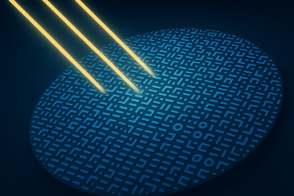
A metalens, by contrast, achieves this without any bulk or curvature. It uses a carefully designed pattern of nanostructures — often sub-wavelength-sized pillars, ridges, or holes — that locally delay the light's phase in a way that mimics (and sometimes surpasses) the bending done by a curved lens. The lens itself can be just a few hundred nanometers thick.
At first glance, it looks like a transparent disk. But zoom in, and you’ll find it’s more like a light-manipulating forest.
How Does It Work? (A Quick Physics Primer)
Metalenses fall under a broader category called metasurfaces — ultrathin, planar structures engineered to control electromagnetic waves in precise ways.
At the heart of a metalens is the ability to impart spatially varying phase shifts to incoming light. Here’s how:
The surface is divided into an array of nanopillars or meta-atoms, each smaller than the wavelength of light.
By adjusting the diameter, height, or material of each nanopillar, we can control how much it delays the phase of the light passing through it.
By arranging these pillars in the right pattern across the surface, we can make the overall lens focus or deflect light — just like a traditional lens, but without the bulk.
If that sounds similar to the idea behind a Fresnel lens or diffractive optics, you’re not wrong — but metasurfaces go further. They offer subwavelength control with fewer aberrations, polarization selectivity, and even multifunctionality (e.g., focusing and filtering at the same time).
Making a Metalens: Where Nanotech Meets Optics
Designing the metalens is only half the battle. The real challenge lies in fabrication — turning a theoretical pattern into a real structure, atom by atom.
Here’s what a typical process might look like:
Substrate Preparation: Start with a clean, transparent substrate like fused silica.
Resist Coating and Lithography: A high-resolution resist is spin-coated, and the desired nanopattern is written using electron beam lithography (EBL) or nanoimprint lithography (NIL). This is where nanolithography tools like the NanoFrazor or advanced e-beam writers come into play.
Etching or Deposition: Depending on the design, we might either etch nanopillars into the substrate or deposit high-index materials (like TiO₂ or silicon) into the resist template.
Lift-Off and Post-Processing: After structuring, we remove the resist and apply any necessary coatings. The result: a precisely engineered forest of nano-objects, ready to bend and shape light.
Each step has trade-offs — higher refractive index materials allow stronger phase shifts with smaller features, but can be harder to etch or deposit uniformly. Likewise, EBL provides unmatched resolution, but is too slow for mass production.
What’s the Big Deal?
Metalenses promise lighter, thinner, cheaper, and potentially smarter optics:
Miniaturization: Flat optics mean slimmer phones, lighter drones, and more compact medical instruments.
Monolithic integration: Metalenses can be fabricated directly onto chips, opening up new possibilities for on-chip imaging or quantum photonics.
New optical functionalities: From achromatic lenses (focusing all colors to the same point) to polarization-sensitive imaging, metasurfaces break the limitations of classical optics.
But the road to commercial adoption is still being paved. Challenges like low efficiency at visible wavelengths, fabrication scalability, and robustness under real-world conditions remain active areas of research.
Beyond the Lens
What excites me most about metalenses isn’t just their flatness. It’s the mindset shift they represent — from shaping bulk materials to shaping light-matter interactions at the nanoscale.
We’re not just polishing glass anymore. We’re engineering phase, polarization, and wavefront directly through design — almost like programming optics.
And as a software engineer working in nanotech, I can’t help but see this as a convergence of disciplines: optics becoming more like code, and nanofabrication as the compiler.


Comments